LTC4222
14
4222fb
APPLICATIONS INFORMATION
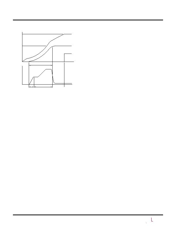
Figure 2. Power-Up Waveform
V
DD
+ 6V
V
GATE
V
OUT
GPIO
(POWER GOOD)
I
LOAD
" R
SENSE
V
DD
V
SENSE
50mV
17mV
SS
LIMITED
FB
LIMITED
4222 F02
TIMER
EXPIRES
t
STARTUP
the output, a 12礎 pull-up current (I
GATE
) from the GATE
pin slews the gate upwards and resulting current is less
than the current limit. Because the inrush current is less
than the current limit, the start-up timer can expire without
producing an overcurrent fault and a small timer capacitor
may be used. After the timer has expired power good will
not be signaled until the FB pin crosses its threshold and
the GATE-to-SOURCE voltage crosses the 4.3V threshold
that indicates the MOSFET is fully enhanced. When both
those conditions are met the output voltage is suitable
for the load to be turned on and the impedance back to
the supply through the MOSFET is low. Power good is
then asserted with the GPIO pin or read via the interface,
signaling that it is safe to turn on downstream loads. A
power-bad fault is not generated when starting up in this
manner because the FB pin will cross its threshold before
the GATE-to-SOURCE threshold is crossed. R
G
should be
chosen such that I
GATE
" R
G
is less than the threshold of
the MOSFET to avoid a current spike at the beginning of
startup. Reducing R
G
degrades the stability of the current
limit circuit, see applications information on current limit
stability.
GATE Pin Voltage
A curve of GATE-to-SOURCE voltage vs V
DD
is shown in
the Typical Performance Characteristics. At minimum input
supply voltage of 2.9V , the minimum GATE-to-SOURCE
drive voltage is 4.7V . The GATE-to-SOURCE voltage is
clamped below 6.5V to protect the gates of logic-level
N-channel MOSFETs.
Turn-Off Sequence
One or both GATE pins are turned off by a variety of con-
ditions. A normal turn-off is initiated by an ON pin going
low or a serial bus turn-off command. Additionally, several
fault conditions cause a GATE to turn off. These include an
input overvoltage (OV pin), input undervoltage (UV pin),
overcurrent circuit breaker (SENSE
pin), or EN transitioning
high. Writing a logic one into the UV , OV or OC fault bits
(FAULT register bits 0 to 2 in Table 6) also latches off the
associated GATE if their auto-retry bits are set to false.
A MOSFET is turned off with a 1mA current pulling down
the GATE pin to ground. With the MOSFET turned off, the
SOURCE and FB voltages drop as C
L
discharges. When
the FB voltage crosses below its threshold, GPIO may be
configured to pull low to indicate that the output power
is no longer good.
If the INTV
CC
pin drops below 2.60V for greater than 1祍,
or the associated V
DD
pin falls below 2.35V for greater than
2祍, a fast shut down of the MOSFET is initiated. In this
case the GATE pin is pulled down with a 450mA current
to the SOURCE pin.
Overcurrent Fault
The LTC4222 has different current limiting behavior during
start-up, when the output supply ramps up under TIMER,
SS and FB control, and normal operation. As such it can
generate an overcurrent fault during both phases of op-
eration. Both set the faulting supplys overcurrent fault bit
(FAULT register bit 2) and shut off the faulting GATE, or
both GATEs if the CONFIG pin is low.
During start-up when both TIMER and SS are ramping,
the current limit is a function of SS pin voltage and the
voltage on the FB pins. A supply could power up entirely
in current limit depending on the bypass capacitor at the
outputs of the ramping supplies. The TIMER pin sets
the time duration for current limit during start-up, either
12.3ms/礔 when using a timer capacitor, or 100ms when
the TIMER pin is tied to INTV
CC
. If the supply is still in
current limit at the end of the timing cycle, an overcurrent
发布紧急采购,3分钟左右您将得到回复。
相关PDF资料
LTC4223CDHD-2#PBF
IC CNTRLR HOT SWAP DUAL 16-DFN
LTC4224IDDB-2#TRPBF
IC CNTRLR HOT SWAP DUAL 10-DFN
LTC4225IGN-1#PBF
IC CONTROLLER HOT SWAP 24-SSOP
LTC4230CGN#TRPBF
IC CONTRLLR HOT SWAP TRPL 20SSOP
LTC4232CDHC#TRPBF
IC CTLR HOT SWAP 5A 16-DFN
LTC4240IGN#TRPBF
IC CTRLR HOTSWAP CPCI I2C 28SSOP
LTC4241IGN#PBF
IC CTRLR HOTSWAP 3.3V AUX 20SSOP
LTC4242CUHF#TRPBF
IC CNTRLR HOT SWAP 38-QFN
相关代理商/技术参数
LTC4222CG#TRPBF
功能描述:IC CTRLR DUAL HOT SWAP 36-SSOP RoHS:是 类别:集成电路 (IC) >> PMIC - 热交换 系列:- 产品培训模块:Lead (SnPb) Finish for COTS
Obsolescence Mitigation Program 标准包装:119 系列:- 类型:热交换控制器 应用:通用型,PCI Express? 内部开关:无 电流限制:- 电源电压:3.3V,12V 工作温度:-40°C ~ 85°C 安装类型:表面贴装 封装/外壳:80-TQFP 供应商设备封装:80-TQFP(12x12) 包装:托盘 产品目录页面:1423 (CN2011-ZH PDF)
LTC4222CG-TRPBF
制造商:LINER 制造商全称:Linear Technology 功能描述:Dual Hot Swap Controller with I2C Compatible Monitoring
LTC4222CUH#PBF
功能描述:IC CTRLR DUAL HOT SWAP 32-QFN RoHS:是 类别:集成电路 (IC) >> PMIC - 热交换 系列:- 产品培训模块:Lead (SnPb) Finish for COTS
Obsolescence Mitigation Program 标准包装:119 系列:- 类型:热交换控制器 应用:通用型,PCI Express? 内部开关:无 电流限制:- 电源电压:3.3V,12V 工作温度:-40°C ~ 85°C 安装类型:表面贴装 封装/外壳:80-TQFP 供应商设备封装:80-TQFP(12x12) 包装:托盘 产品目录页面:1423 (CN2011-ZH PDF)
LTC4222CUH#TRPBF
功能描述:IC CTRLR DUAL HOT SWAP 32-QFN RoHS:是 类别:集成电路 (IC) >> PMIC - 热交换 系列:- 产品培训模块:Lead (SnPb) Finish for COTS
Obsolescence Mitigation Program 标准包装:119 系列:- 类型:热交换控制器 应用:通用型,PCI Express? 内部开关:无 电流限制:- 电源电压:3.3V,12V 工作温度:-40°C ~ 85°C 安装类型:表面贴装 封装/外壳:80-TQFP 供应商设备封装:80-TQFP(12x12) 包装:托盘 产品目录页面:1423 (CN2011-ZH PDF)
LTC4222CUH-PBF
制造商:LINER 制造商全称:Linear Technology 功能描述:Dual Hot Swap Controller with I2C Compatible Monitoring
LTC4222CUH-TRPBF
制造商:LINER 制造商全称:Linear Technology 功能描述:Dual Hot Swap Controller with I2C Compatible Monitoring
LTC4222IG#PBF
功能描述:IC CTRLR DUAL HOT SWAP 36-SSOP RoHS:是 类别:集成电路 (IC) >> PMIC - 热交换 系列:- 产品培训模块:Lead (SnPb) Finish for COTS
Obsolescence Mitigation Program 标准包装:119 系列:- 类型:热交换控制器 应用:通用型,PCI Express? 内部开关:无 电流限制:- 电源电压:3.3V,12V 工作温度:-40°C ~ 85°C 安装类型:表面贴装 封装/外壳:80-TQFP 供应商设备封装:80-TQFP(12x12) 包装:托盘 产品目录页面:1423 (CN2011-ZH PDF)
LTC4222IG#TRPBF
功能描述:IC CTRLR DUAL HOT SWAP 36-SSOP RoHS:是 类别:集成电路 (IC) >> PMIC - 热交换 系列:- 产品培训模块:Lead (SnPb) Finish for COTS
Obsolescence Mitigation Program 标准包装:119 系列:- 类型:热交换控制器 应用:通用型,PCI Express? 内部开关:无 电流限制:- 电源电压:3.3V,12V 工作温度:-40°C ~ 85°C 安装类型:表面贴装 封装/外壳:80-TQFP 供应商设备封装:80-TQFP(12x12) 包装:托盘 产品目录页面:1423 (CN2011-ZH PDF)